FDE Solver
Solver Physics
The Finite-Difference Eigenmode (FDE) solver obtains the field distribution, effective refractive index, and loss of waveguide modes by solving Maxwell's equations using a finite-difference mesh algorithm on the cross-section of the waveguide. Additionally, the integrated frequency sweep tool allows for easy extraction of results such as group delay and dispersion. Moreover, this solver is capable of handling curved waveguide structures.
 |
|---|
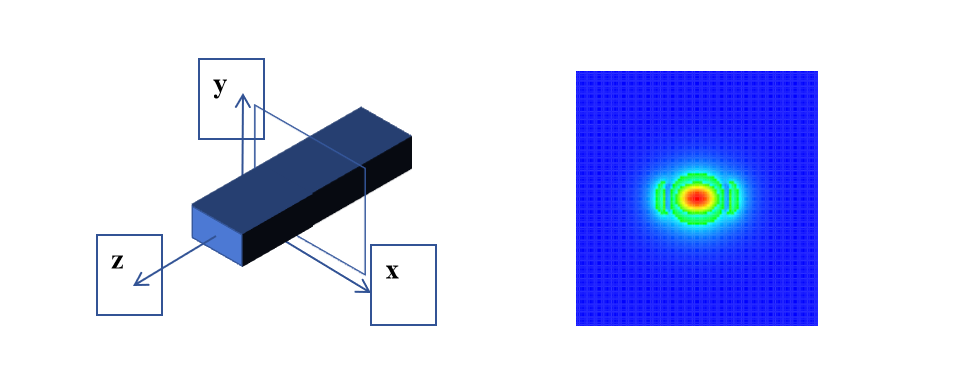
Assuming the invariant waveguide is along the axial direction 𝑧, the electromagnetic field distribution of any waveguide mode can be expressed in the following form:
Here, , denotes the corresponding second-order partial differential operator. This operator is related to the material properties distribution across the waveguide cross-section. The corresponding magnetic field characteristic equation is similar.
In the FDE solver, we establish a 2D mesh on the cross-section of the waveguide and discretizes the aforementioned characteristic equation, which includes the electric field , and the operator , using finite difference method. This results in discretized characteristic equations that the waveguide modes must satisfy. By numerically solving this characteristic equation, the field distributions and of the corresponding waveguide modes, as well as the square of the propagation constant , can be obtained.
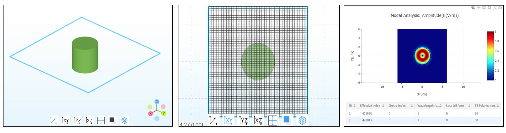
As shown in the figure below, fig(left) displays the structure and the FDE region, fig(middle) illustrates the grid discretization of the mode-solving(FDE) plane, fig(right) presents the results of the mode solving.
 |
|---|
Note: The propagation constant 𝛽 can be obtained by taking the square root. If the waveguide material does not have gain, the square root should be chosen such that the imaginary part of 𝛽 is zero or negative. A positive imaginary part corresponds to evanescent or radiative (decaying) modes, while the real part indicates the propagation direction of the waveguide mode.
The accuracy of the FDE solver improves with an increase in the transverse grid density. However, this comes at the cost of significantly increased computational effort. Using mesh refinement allows for high-accuracy mode calculations even with relatively sparse grids. Additionally, adaptive mesh refinement can be employed, where finer local grids are used in regions with complex material structures, achieving higher accuracy without a substantial increase in computational load.
Features Description
Add or edit a FDE simulation area and boundary conditions.
Settings Description
In this section, we show how to use Max-Optics to run FDE simulation and view the simulation result.
1 General
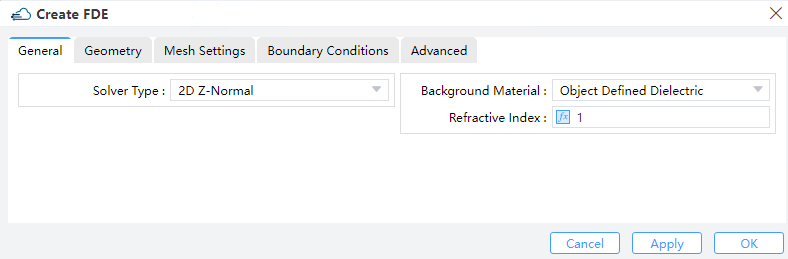 |
|---|
1) Solver Type: 2D X-Normal/Y-Normal/Z-Normal, 1D X: Y/Z Prop, 1D Y:X/Z Prop. (Default: 2D Z-Normal)
2) Background Material: The combo box allow user to set the background material from drop down menu. Project, Object Defined Dielectric, and Go to Material Library can be operated.
Project: Materials that have been imported into the project can be selected and used as background media in simulation. We can also select "Object Defined Dielectric" to customize the background material index in the refractive index.
- Object Defined Dielectric: The object defined dielectric material, a default setting if user forgets to set background material, is defined for the current object background material setting. Once users chooses this option, they does not need to set any material from the standard, user, or project material database. And the object-defined dielectric will not be loaded into any material database.
- Refractive Index: specify background index manually in stead of choosing form library or project. (Default :1).
- Object Defined Dielectric: The object defined dielectric material, a default setting if user forgets to set background material, is defined for the current object background material setting. Once users chooses this option, they does not need to set any material from the standard, user, or project material database. And the object-defined dielectric will not be loaded into any material database.
Go to Material Library: If selected, user can go to standard material database to set background material according to needs. The selected material will be imported into the project automatically.
2 Geometry
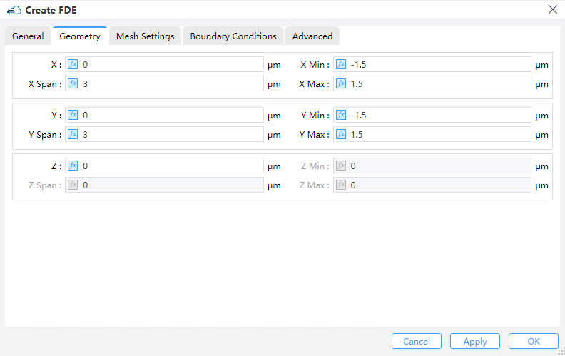 |
|---|
1) X, Y, Z: The center of the simulation region.
2) X Min, X Max: minimal and maximal.in x direction
3) Y Min, Y Max: minimal and maximal.in y direction.
4) Z Min, Z Max: minimal and maximal.in z direction
5) X Span, Y Span, Z Span: X, Y, Z span of the simulation region. (Notes: The availability is based on the solver type.)
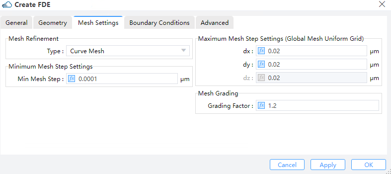
3 Mesh Settings
 |
|---|
1) Mesh Refinement: Decide the type of mesh refinement, the default selection is Curve Mesh.
- Curve Mesh: The effective permittivity can be derived using the contour path formula, which effectively takes into account the shape of the dielectric interface as well as the weighting of the material filling ratio within the mesh.
- Staircase: It is possible to compute any point within the Yee grid to determine which material it is filled with, and the properties of that single material are used to describe the E-field at that point.As a result, the discrete structure can barely account for the structural variations within a single Yee grid, leading to a Staircase dielectric constant mesh that is fully consistent with the Cartesian grid. Moreover, all layers are effectively moved to the closest E-field position within the Yee grid, meaning that thicknesses cannot be resolved to finer than dx, and thus, cannot be resolved better than dx.
2) Maximum Mesh Step Settings:dx/dy/dz: Maximum mesh step settings in x/y/z direction. The default value is 0.02 μm.
3) Minimum Mesh Step Settings: This indicates the minimum mesh step in the whole simulation region(including also the mesh override regions). (Default: 0.0001μm)
4) Mesh Grading: Grading Factor : In the case of a non-uniform mesh, Mesh Grading specifies the maximum ratio at which a neighboring grid can be enlarged or reduced. (Default: 1.2)
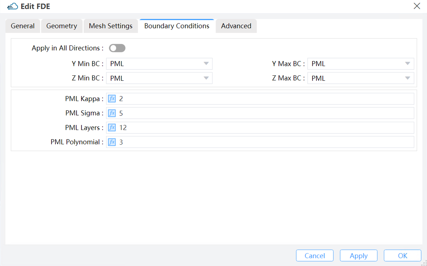
4 Boundary Conditions
 |
|---|
1) Apply in All Directions: Turning on this switch ensures that the boundary conditions are consistent in different directions.
2) PML(Perfect Matched Layer): Electromagnetic waves incident on the Perfect Matched Layer (PML) boundary will be completely absorbed, effectively simulating an ideal open (or non-reflecting) boundary. Compared to traditional boundary conditions, PML boundaries occupy a finite volume around the simulation region, thus having only a limited thickness where the light absorption process occurs.
PML Layers: For discretization purposes, the PML region is divided into multiple layers.
Kappa, Sigma: To control the absorption performance of the PML boundary according to simulation needs, Kappa and Sigma are used. As referenced, Kappa is dimensionless by definition, while Sigma needs to be normalized to be entered as a dimensionless value in the PML settings table. Specifically, both Kappa and Sigma are evaluated through polynomial variations based on their geometric positions within the PML region.
PML Polynomial: This specifies the order of the polynomial used for grading Kappa and Sigma.
2) PEC(Perfect Electric Conductor): The PEC boundary condition is introduced to simulate boundaries that behave as perfect electric conductor. Metal boundaries reflect all electromagnetic waves, thus preventing any energy from passing through the simulation volume enclosed by the metal.
3) PMC(Perfect Magnetic Conductor): Perfect Magnetic Conductor boundary conditions are introduced to be the magnetic correspondence of the metal (PEC) boundaries.
4) Symmetry/Anti-symmetry: Symmetry/Anti-symmetry boundary conditions are often used when studying systems that exhibit one or more symmetry axes or planes, applied to both structures and sources. For the electric field, symmetry boundaries act as mirrors, while anti-symmetry boundaries act as anti-mirrors. Conversely, for the magnetic field, the situation is reversed. The choice between symmetry and anti-symmetry boundary conditions is often crucial for the required vector symmetry of the solution. Note that sources and boundary conditions must utilize the same type of symmetry for the results to be meaningful.
5) Periodic: If the system of interest exhibits spatial periodicity to some extent, periodic boundary conditions (BCs) allow us to analyze the entire system by studying just one repeating unit. By setting up a simulation span that matches the length of the repeating structure and selecting Periodic BCs for that boundary, we can easily enable this condition. As a result, throughout the simulation, the electromagnetic fields on one side of the structure (affected by the periodic BC) are consistently replicated on the opposite side.
Notes: It is crucial to keep in mind that when employing periodic boundary conditions, both the physical structure and the electromagnetic (EM) fields in the system must be periodic. Neglecting this key aspect often leads to errors, such as utilizing PBCs in systems with a periodic structure but non-periodic EM fields.
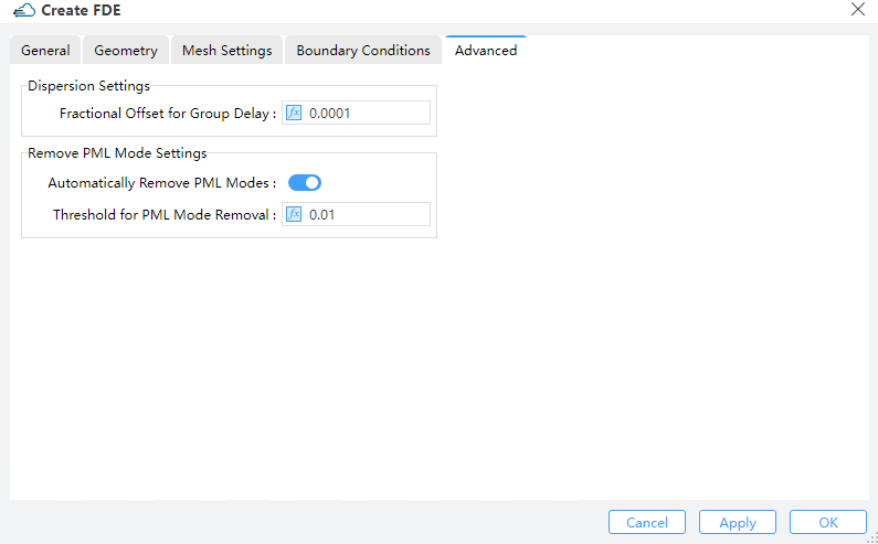
5 Advanced
 |
|---|
1) Fractional Offset for Group Delay: Numerically, the group delay of the device is computed by means of a finite-difference approximation of diffentiating the phase with respect to frequency. The “fractional offset for group delay” refers to the fractional amount of the frequency used in the step size of finite difference. If this setting is too small, the phase change may be severely affected by noise, whereas a too large setting could result in an unrealistic group delay since the phase may change by more than 2π. For rather long devices (10000+ wavelengths) in which the phase varies quickly with frequency, the user is encouraged to reduce this setting from the default value. Otherwise the default setting is generally recommended. (Default:0.0001 μm)
2) Remove PML Mode Settings:
Automatically Remove PML Modes: Decide whether to remove modes in the PML boundary condition.
Threshold for PML Mode Removal: Set the threshold for mode removal.(Default is 0.01).Under the PML boundary condition, if the fraction of magnetic field intensity is larger than this threshold, the modes will be removed .